- 您现在的位置:买卖IC网 > Sheet目录3820 > PIC16C74B-04I/P (Microchip Technology)IC MCU OTP 4KX14 A/D PWM 40DIP
139
SAM7S Series [DATASHEET]
6175M–ATARM–26-Oct-12
20.3.4.1
Flash Read Command
This command is used to read the Flash contents. The memory map is accessible through this command. Memory
is seen as an array of words (32-bit wide). The read command can start at any valid address in the memory plane.
This address must be word-aligned. The address is automatically incremented.
20.3.4.2
Flash Write Command
This command is used to write the Flash contents. The address transmitted must be a valid Flash address in the
memory plane.
The Flash memory plane is organized into several pages. Data to be written is stored in a load buffer that corre-
sponds to a Flash memory page. The load buffer is automatically flushed to the Flash:
before access to any page than the current one
at the end of the number of words transmitted
The Write Page command (WP) is optimized for consecutive writes. Write handshaking can be chained; an inter-
nal address buffer is automatically increased.
Flash Write Page and Lock command (WPL) is equivalent to the Flash Write Command. However, the lock bit is
automatically set at the end of the Flash write operation. As a lock region is composed of several pages, the pro-
grammer writes to the first pages of the lock region using Flash write commands and writes to the last page of the
lock region using a Flash write and lock command.
Flash Erase Page and Write command (EWP) is equivalent to the Flash Write Command. However, before pro-
gramming the load buffer, the page is erased.
Flash Erase Page and Write the Lock command (EWPL) combines EWP and WPL commands.
20.3.4.3
Flash Full Erase Command
This command is used to erase the Flash memory planes.
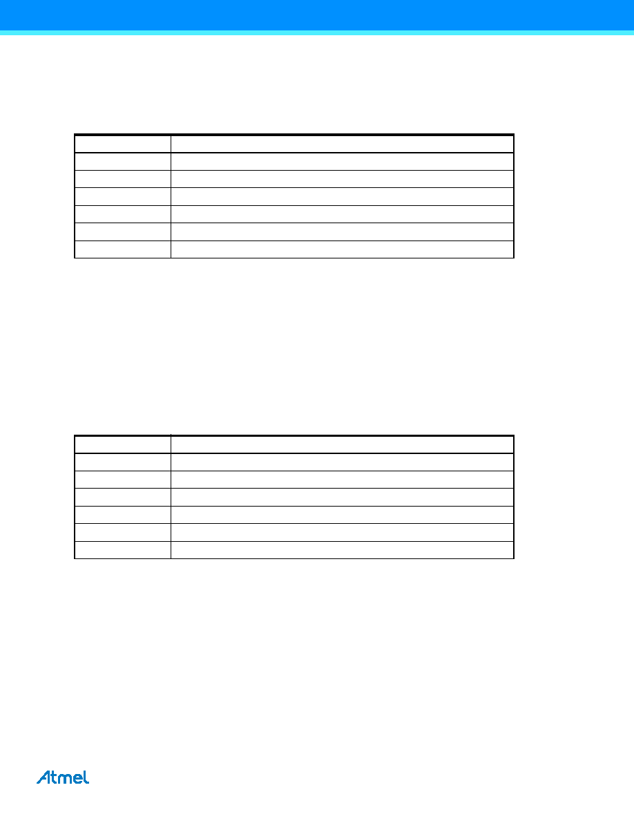
Table 20-22. Read Command
Read/Write
DR Data
Write
(Number of Words to Read) << 16 | READ
Write
Address
Read
Memory [address]
Read
Memory [address+4]
...
Read
Memory [address+(Number of Words to Read - 1)* 4]
Table 20-23. Write Command
Read/Write
DR Data
Write
(Number of Words to Write) << 16 | (WP or WPL or EWP or EWPL)
Write
Address
Write
Memory [address]
Write
Memory [address+4]
Write
Memory [address+8]
Write
Memory [address+(Number of Words to Write - 1)* 4]
发布紧急采购,3分钟左右您将得到回复。
相关PDF资料
C8051F236R
IC 8051 MCU 8K FLASH 48TQFP
C8051F231R
IC 8051 MCU 8K FLASH 32LQFP
C8051F230R
IC 8051 MCU 8K FLASH 48TQFP
608017032300339
CONTACT CRIMP RACK & PANEL
516-290-541
CONTACT RACK & PANEL WIREWRAP
516-290-500
CONTACT RACK & PANEL SOLDER EYE
516-290-520
CONTACT RACK & PANEL SOLDERTAIL
516-290-590
CONTACT RACK & PANEL CRIMP
相关代理商/技术参数
PIC16C74B-04I/P
制造商:Microchip Technology Inc 功能描述:IC 8BIT CMOS MCU 16C74 DIP40
PIC16C74B-04I/PQ
功能描述:8位微控制器 -MCU 7KB 192 RAM 33 I/O RoHS:否 制造商:Silicon Labs 核心:8051 处理器系列:C8051F39x 数据总线宽度:8 bit 最大时钟频率:50 MHz 程序存储器大小:16 KB 数据 RAM 大小:1 KB 片上 ADC:Yes 工作电源电压:1.8 V to 3.6 V 工作温度范围:- 40 C to + 105 C 封装 / 箱体:QFN-20 安装风格:SMD/SMT
PIC16C74B-04I/PT
功能描述:8位微控制器 -MCU 7KB 192 RAM 33 I/O RoHS:否 制造商:Silicon Labs 核心:8051 处理器系列:C8051F39x 数据总线宽度:8 bit 最大时钟频率:50 MHz 程序存储器大小:16 KB 数据 RAM 大小:1 KB 片上 ADC:Yes 工作电源电压:1.8 V to 3.6 V 工作温度范围:- 40 C to + 105 C 封装 / 箱体:QFN-20 安装风格:SMD/SMT
PIC16C74B-20/L
功能描述:8位微控制器 -MCU 7KB 192 RAM 33 I/O RoHS:否 制造商:Silicon Labs 核心:8051 处理器系列:C8051F39x 数据总线宽度:8 bit 最大时钟频率:50 MHz 程序存储器大小:16 KB 数据 RAM 大小:1 KB 片上 ADC:Yes 工作电源电压:1.8 V to 3.6 V 工作温度范围:- 40 C to + 105 C 封装 / 箱体:QFN-20 安装风格:SMD/SMT
PIC16C74B-20/L
制造商:Microchip Technology Inc 功能描述:8BIT CMOS MCU SMD 16C74 PLCC44
PIC16C74B-20/P
功能描述:8位微控制器 -MCU 7KB 192 RAM 33 I/O RoHS:否 制造商:Silicon Labs 核心:8051 处理器系列:C8051F39x 数据总线宽度:8 bit 最大时钟频率:50 MHz 程序存储器大小:16 KB 数据 RAM 大小:1 KB 片上 ADC:Yes 工作电源电压:1.8 V to 3.6 V 工作温度范围:- 40 C to + 105 C 封装 / 箱体:QFN-20 安装风格:SMD/SMT
PIC16C74B-20/P
制造商:Microchip Technology Inc 功能描述:IC 8BIT CMOS MCU 16C74 DIP40
PIC16C74B-20/PQ
功能描述:8位微控制器 -MCU 7KB 192 RAM 33 I/O RoHS:否 制造商:Silicon Labs 核心:8051 处理器系列:C8051F39x 数据总线宽度:8 bit 最大时钟频率:50 MHz 程序存储器大小:16 KB 数据 RAM 大小:1 KB 片上 ADC:Yes 工作电源电压:1.8 V to 3.6 V 工作温度范围:- 40 C to + 105 C 封装 / 箱体:QFN-20 安装风格:SMD/SMT